This page contains more information about our presentation “Developing AlMn films for Argonne TES fabrication,” for the 18th International Workshop on Low Temperature Detectors, in Milan, Italy, 22-26 July 2019.
Promotional video:
Full poster (#200) as presented at LTD18. Link to PDF version here
Abstract: The reference design for the next-generation cosmic microwave background (CMB) experiment, CMB-S4, relies on large arrays of transition edge sensor (TES) bolometers coupled to Superconducting Quantum Interference Device (SQUID)-based readout systems. Mapping the CMB to near cosmic variance limits will enable the search for signatures of inflation and constrain dark energy and neutrino physics. AlMn TESes provide simple film manufacturing and highly uniform arrays over large areas to meet the requirements of the CMB-S4 experiment. TES parameters such as critical temperature and normal resistance must be tuned to experiment specifications and can be varied based on geometry and steps in the fabrication process such as deposition layering, geometry, and baking time and temperature. Using four-terminal sensing, we measured Tc and Rn of AlMn 2000 ppm films and devices of varying thicknesses fabricated at Argonne National Laboratory to motivate device geometries and fabrication processes to tune Tc to 150-200 mK and Rn to ~10 mOhms. Measurements of IV curves and time constants for the resulting devices of varying leg length were made using time-division SQUID multiplexing, and determined Tc, G, k, f3db, and Rn. We present the results of these tests along with the geometries and fabrication steps used to tune the device parameters to the desired limits.
Motivation: The cosmic microwave background (CMB) contains a wealth of information about the origins, evolution, and fundamental physics of our universe. CMB-S4 is a proposed “Stage-4” ground-based CMB experiment that will map the polarization of the CMB in multiple frequency bands to nearly the cosmic variance limit. CMB-S4 targets science goals that include characterizing dark energy and dark matter, searching for signatures of inflation in the early universe, measuring the sum of the neutrino masses, and mapping the universe’s matter distribution.
You can learn more about CMB-S4 here:
CMB-S4 Science Case, Reference Design, and Project Plan
CMB-S4 will rely on large arrays of Transition-Edge Sensors (TESes) coupled to Superconducting Quantum Interference Device (SQUID)-based readout systems to reach its sensitivity target. TESes are a mature technology and have been thoroughly demonstrated to achieve CMB science goals. TESes are also scalable, enabling the order of magnitude higher detector counts required by CMB-S4. The choice of AlMn TESes will provide CMB-S4 with simple film manufacturing and highly uniform distributions of device parameters over large arrays.
Monolithic arrays of multichroic TESes have been previously fabricated at Argonne National Laboratory and deployed in the South Pole Telescope’s SPT-3G camera. These Ti/Au bolometers have a critical temperature of Tc = 420 mK and a normal resistance of Rn = 2 Ohms. To meet the experiment design requirements for CMB-S4, AlMn2000ppm TES fabrication will target a Tc ~ 150-200 mK and an Rn ~ 10-20 mOhms. While SPT-3G used a 3He absorption refrigerator with a bath temperature of ~250 mK, CMB-S4 will use dilution refrigerators with bath temperatures < 100 mK. Reducing the bath temperature will reduce the thermal fluctuation noise. Reducing Rn will optimize the detector arrays for TDM or uMUX readout. The fabrication process at Argonne will therefore need to be tuned to achieve these device parameters. Variables in the fabrication process such as the Mn concentration, thickness and geometry of films, thermal annealing temperature, and presence of additional material layers all affect the AlMn device parameters and must be tuned to meet specifications through repeated rounds of test fabrication and testing.
Learn more:
Fabrication of TESes for SPT-3G
Design and characterization of the SPT-3G receiver
Fabrication:
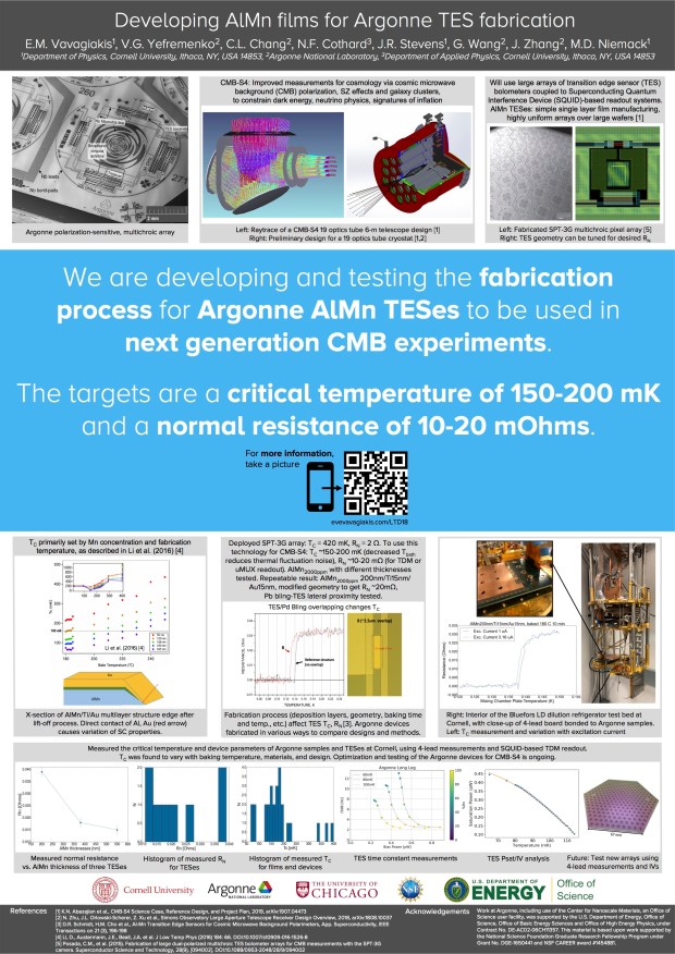
Film samples and devices were fabricated at Argonne National Laboratory and tested at Cornell University to develop the fabrication process. Bare film studies were performed to study the impact of substrate choice and Ti (or Mo) buffer layer between AlMn and Au depositions. A film stack of 2000ppm AlMn on SiO2 with a Ti15/Au15 top layer was chosen based on good critical temperature repeatability and was derived from the Ti/Au SPT-3G array fabrication. The top layer of Au was chosen to prevent oxidation and protect the underlying films, while remaining conductive to connect leads to the device from the top side of fabrication. Patterned films were then tested to predict device Tc and Rn.
The thickness and aspect ratio of the film stacks was then iterated upon to target the desired Rn. Baking time and temperature was selected to target Tc. A lift-off process is used for TES patterns, which can potentially lead to tapered edges and interaction between the Al and Au layers, and thus to poor transitions for thicker films. Such edge effects as well as proximity effects were considered while iterating on patterned films and TESes.
A. Cross section of Al/Au bilayer. Direct contact of Al and Au leads to the formation of intermetallic compounds and the variation of superconducting properties. B. Cross section of AlMn/Ti/Au multilayer structure edge after the lift-off process. Red arrow indicates an area of possible AlMn-Au direct contact, depending on the thickness of the layers. Such contact can cause a poor superconducting transition.
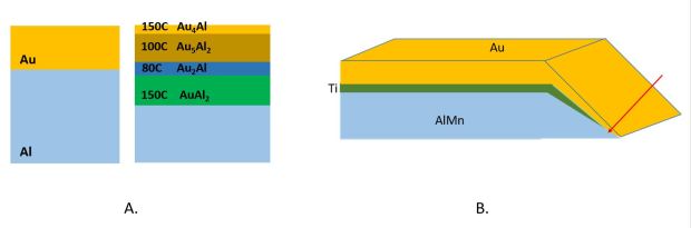
A modified SPT-3G TES island. AlMn200nm/Ti15nm/Au15nm TES film is 15 um long by 80 um wide.
Testing: Samples were wire bonded and affixed with rubber cement to a printed circuit board (PCB) and mounted to the coldest (100 mK) stage of a dilution refrigerator (DR) with an internal 300 K magnetic shield. Four-lead measurements were taken of the samples, which precisely measure low resistance values by eliminating the lead and contact resistances from the measurements. Temperature was varied as resistances were logged via a Lakeshore AC resistance bridge, reading out the superconducting transition and measuring Tc and Rn For each transition, Tc was taken to be the temperature value at 50% Rn, where Rn is the resistance value measured at 2 mK above the last superconducting data point in the resistance versus temperature curve. Excitation currents were varied to ensure their choice didn’t significantly affect the measured Tc. The total error on Tc is taken to be 2 mK, and the error on Rn to be 0.02 Ohms.
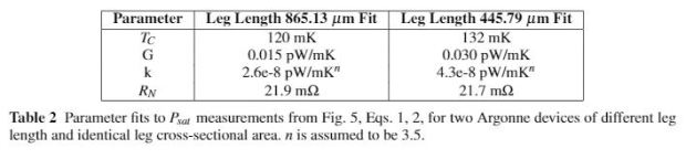
Fabricated TESes of two different leg lengths of equal cross-sectional area, 865.13 um and 445.79 um were mounted to a PCB on the cold stage of the DR, and read out using the same time division multiplexing (TDM) system used in AdvACT with NIST SQUIDs. TDM measurements of current-voltage (IV) curves at various bath temperatures were aquired for a “long” and “short” leg length AlMn2000 200nm/Ti15nm/Au15nm TES.
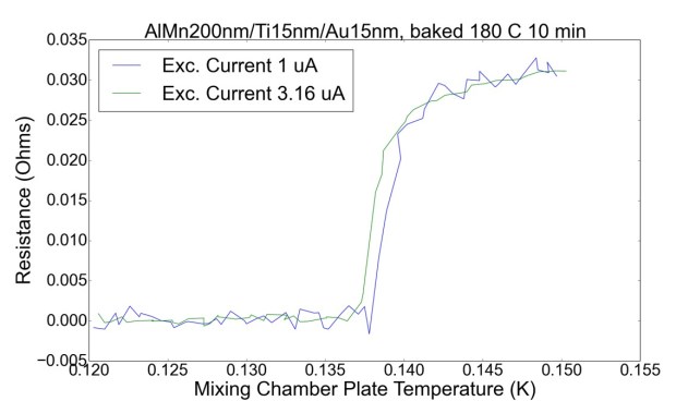
Example of the four-lead R vs. T measurement of a film superconducting transition. Choice of excitation current influences results, and Tc is recorded for an excitation current which has been reduced enough to keep Tc consistent within 2 mK.
Results: The results of the four-lead measurements are summarized in the following table:
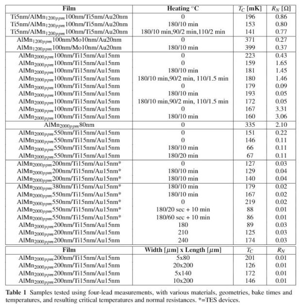
Results of four-lead measurements. A: Critical temperature vs. annealing temperature for three AlMn2000ppm 200nm/Ti15nm/Au15nm films along with linear fit showing the effect of baking on Tc. B: Normal resistance vs. AlMn thickness in nm for three film samples, showing Rn decreasing with increasing material thickness. C: Histogram of all Argonne sample critical temperatures measured at Cornell, highlighting a trend of narrowing in on the desired critical temperature of 150-200 mK for CMB-S4.

Saturation power versus temperature along with fits to Psat measurements for two devices. Left: Argonne short leg length (445.79 um) TES, with optimal n fixed at 2.76. Right: Argonne long leg length (865.13 um) TES, with optimal n fixed at 2.91. Optimal n is defined as the value of n which minimizes the chi-square goodness-of-fit to Psat.
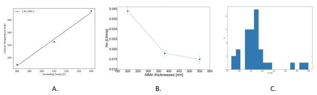
Results of bias step measurements. f3dB versus bias power in pW for four bath temperatures. Left: Argonne short leg length (445.79 um) TES. Right: Argonne long leg length (865.13 um) TES.
Next steps: We have measured Tc, G, k, f3db, and Rn for two Argonne AlMn TESes, and Tc and Rn for various film stacks to motivate the selection of materials, thickness, geometry, and bake time and temperature. Through iterative testing, we inform Argonne’s fabrication process to produce TESes which have the desired critical temperature (150-200 mK) and normal resistance (10-20 mOhms) to be used for precision measurements of the CMB in the next-generation CMB experiment, CMB-S4. Next steps include acquiring noise data for the Argonne devices and eventually testing full wafers.
